Solder wire and paste feature | SMT Technology
Solder voiding is present in the majority solder joints and is generally accepted when the voids are small and the total void content is minimal. X-ray methods are the predominate method for solder void analysis but this method can be quite subjective for non grid array components due to the two dimensional aspects of X-ray images and software limitations. A novel method of making a copper “sandwich” to simulate under lead and under component environs during reflow has been developed and is discussed in detail. This method has enabled quantitative solder paste void analysis for lead free and specialty paste development and process refinement. Profile and paste storage effects on voiding are discussed. Additionally an optimal design and material selection from a solder void standpoint for a heat spreader on a BCC (Bumpered Chip Carrier) has been developed and is discussed.
Solder voids in solder joints are a common occurrence in SMT assemblies. Their origins are not well understood but are typically faulted as a failure of the solder fillet to thoroughly expel flux remnants during the reflow process. The amount of solder voiding can vary significantly within an assembly, between different flux formulations, solder alloys, board and component metalizations. Reflow profiles as well as stencil aperture designs can often affect the overall level of voiding.
Adding to the mystery of solder voiding is a lack of quantitative measurement tools in the industry with few exceptions. BGA void analysis software is one of these exceptions. This software uses gray level pixel analysis to determine the perimeter of the solder sphere and the internal perimeters of the voids. Once the perimeters are established the areas within these structures can be measured and an overall percent voiding can be calculated. This type of measurement works well if the voids are large or found on the outer edges of the sphere but if the void is small and centrally located where the sphere density is the greatest then the void may be invisible due to its relatively similar gray level to the surrounding material. Increasing the X-ray power will reveal the small void but also shrink the measured area of the sphere and yield an inaccurate and inflated percent voiding. This problem is even more complicated in a chip or a leaded component solder joint. When X-raying a completed assembly, internal traces, vias and even components on the backside of the board that intersect the image of the solder joint confound the software algorithms ability to accurately determine the perimeter of the solder joint. In simple terms the X-ray image is two-dimensional and the ideal structure must be symmetrical about the Z-axis such as a box or a cylinder.
Novel Approach
Based on the assumption that the ideal quantitative void measurement method will utilize BGA analysis software and a symmetrical Z-axis reflow structure, the “sandwich” concept was developed.
This a novel approach simulates the worst conditions of a solder joint for voiding, under the component where flux evacuation is the most difficult while maintaining the same reflow thermal environment and metallurgies if desired. This idea was born out of a quest for a quantitative method of determining the percent voiding on a Ceramic Column Grid Array (CCGA)1. In the CCGA the columns are 10/90 Sn/Pb and cover about 45% of the solder fillet. If enough power is used to see through these dense columns, the perimeter of the solder joint is washed out and 55% of the total fillet is invisible. If adequate power is used to see the perimeter of the circular fillet, the area under the columns is invisible. The effort is complicated by column parallax, internal traces and vias as can be seen in Figure 1. With the thought of a column the same diameter as the solder pad that is thin enough to be X-rayed without excessive power, a solder preform was selected. In this application the preform alloy was selected to be the same as the 10/90 columns to minimize the variables that could contribute to solder voiding. Several thicknesses were tested with a 30 mil diameter by 5 mil thick as the final solution.
There were numerous challenges placing these discs. The first problem was a reliable source cup shaped and stacked discs were the first problems to solve. The second problem was the mechanics of actually placing the discs in that the vision systems in the pick and place were never programmed to recognize round components, only components with corners like typical chips. This relegated a “ballistic” pick and place strategy. For this problem a precision matrix tray with cylindrical pockets, each holding one preform, was developed as in Figure 2. Next came improvements to the pick and place nozzle. The stock smallest nozzle OD was the same as the preform. This presented numerous pick problems if the preform was not perfectly centered, occasionally the preform would flip on its edge after pick and crash on placement deforming the preform. Several improvements were made ultimately reducing the nozzle tip down to what would be typical for a 0201 chip as in Figure 3. Reducing the nozzle tip surface area helped eject the preform better in the placement operation.
Assembly of the CCGA test coupons is simple SMT assembly beginning with a “pads only” ceramic coupon to maintain the geometries and pad metalization of the application. This coupon is free of internal traces as in Figure 4. The solder paste is printed through a circular aperture that is 1 mil smaller in diameter than the pad, the preform is placed over the solder paste and then reflowed as in Figure 5. It was established that if the preform was off pad less than 4 mils that it would self-center. Careful attention to Z-axis placement is required to prevent shorting with adjacent preforms.
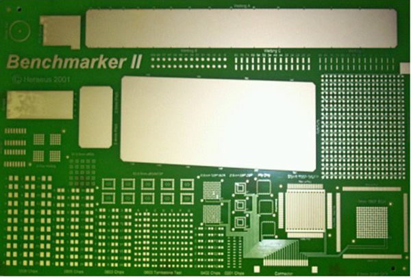
After assembly the coupon area was X-rayed and quantitative void analysis was performed on the image using off- the-shelf BGA analysis software as in Figure 6. This software provides both total percent voiding and a pass/fail status if any individual void within a structure is larger than a preset number (ie 5%). This technique worked very well for the custom formulated 63/37 Sn/Pb based solder paste or any other alloy with a similar melt point but when tested with lead free (Sn/Ag/Cu, Mp 219°C) it was noticed that the preforms had appeared to melt and partially join the underlying solder paste under test. This was remedied by switching to OFHC copper preforms of identical geometries. For generic paste void benchmarking2 a dedicated pad test area (Figure 7) was included in the Benchmarker II test board. This allows the testing of solder pastes on standard PCB surfaces such as Entek OSP (Organic Solder Protectant) and ENIG (Electroless Nickel Immersion Gold). Quite simply we are making copper sandwiches (Figure 8) that result in cylindrical structures, which permit highly quantitative void analysis with standard BGA analysis software.
rom this data there are clearly different trends for the two materials as well as a significant difference in void behavior between them. The effect of time on Material A is accelerated in cold storage and just the opposite with Material B. Both materials have the exact same source and specifications of the inorganics (powder + additives).
Profile Effects
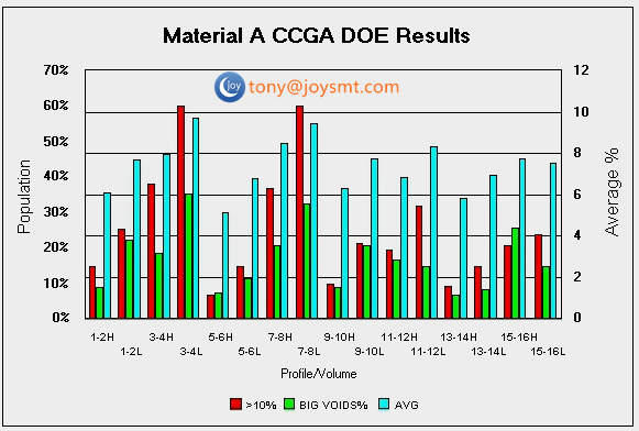
The effect of the reflow profile can be significant but the magnitude varies greatly from one formulation to another. The following example involves two 63/37 Sn/Pb no clean materials3,4, tested over Entek passivated copper using the copper preforms with the 4 profiles as illustrated in Figure 10. This profile matrix is designed to expose profile sensitivity of a given formulation, in this case relating to voiding. There are two profiles with a ramp style preheat and two with a soak preheat. There are 2 profiles with a peak of 225°C with 60 seconds over liquidous and two hotter profiles with a peak of 240°C with an extended liquidous of 90 seconds. The X-ray data has been compressed into a single “point scale” to facilitate comparisons. These points (100 is best) are calculated .


 Panasonic CM202 CM402 CM602 NPM Nozzle 110 115 KXFX0383A00
 Samsung SM320 IC tray
 YAMAHA FEEDER CALIBRATION JIG