Quality Improvement and Enhanced Flexibility Modern Selective Soldering Process Technology
The Turck Group of companies counts amongst the world-wide leading specialists for sensors, interface- and field bus components in the area of industrial automation.
The manufacturing plant in the Erzgebirge (Ore Mountains in English, a mountain range between Germany and the Czech Republic) was established and is dedicated to the distribution, development and manufacture of customer specific electronics marketed under the brand name of Turck-Duotec.
It is in this factory that Turck-Duotec has invested in a further selective soldering system of the newest generation from ERSA. This new VERSAFLOW 3 will support the VERSAFLOW 2, which operates already since 2006, in satisfying the increased output requirement due to the ever rising number of applications. Today, many of our products could not be manufactured cost effectively at the required quality standards without the selective soldering process technology. The needs and the high quality standards of the Duotec customers therefore necessitated the decision to invest in a new flexible selective soldering system
The competition in the EMS sector has considerably intensified over the last few years,. The enormous pressure to reduce production costs, which every service provider today has to face, frequently forces the organization to have a critical look at their established manufacturing structure and manufacturing methods. Turck-Duotec has successfully confronted these challenges on an ongoing basis, and, through continuous optimization of the production flow and methods, has been able to further extend their technological and commercial advantages.
This decision was decisively influenced by the persistent demands of their customers for cost reductions, while at the same time insisting on further quality improvements and shorter lead times for their orders.
Despite all this, in the final result it was the quality aspects that have made selective soldering an irreplaceable part of the manufacturing process. Where clearly defined processes and parameters and their repeatability are demanded, hand soldering is clearly not the process of choice or even an alternative. The results are virtually not reproducible, since they are dependent on the subjective ability and viewpoints of the individual operator. In addition, the results of the hand soldering process will vary because of the wear of the tip of the iron. And finally, the optical appearance of the solder joint is critical, since for the viewer of the final products it is not possible to differentiate between a purposefully made hand soldered joint and a reworked solder joint.
Equally critical to view is the use of special dedicated solder masks, which cover the SMD components on the solder side and only leave open those spaces that are populated with through- hole components which are soldered on a standard wave soldering system.
These masks need to be designed and sourced at a high cost. Provided that they are even possible, later changes or modifications to the masks carry enormous additional costs. Handling of these masks in the production environment is cumbersome, and they require regular cleaning.
From the point of view of quality and long term reliability of the product, another issue may become critical. In the fluxing process of a wave soldering system using these masks, flux very frequently creeps between board underside and the mask itself. This flux is shielded by the mask and does not get in contact with the liquid solder of the wave. As a result, active flux residues may remain on the assembly after wave soldering. The danger of this flux residue lies in a possible reciprocity with remains of the solder paste of the previous SMD reflow process. Depending on the operating conditions of the product in the filed, the existence of detrimental long term effects cannot be excluded.
Decision for the Selective Soldering Process
Modern selective soldering technology offers for these challenges clear and conclusive solutions. The flux required is applied very precisely only to the area where a solder joint is to be made.
Adjacent areas will not be contaminated.
The soldering parameters can, on account of the program controlled mode of operation, be individually tailored to the joint to be made. This high level of flexibility of the parameterization is a substantial step in the direction of “zero-defect soldering”.
At the same time and viewed over the last few years, the SMT layouts became more and more tight. In addition, new component types brought to market are no longer suitable for the wave soldering process. For these, only the reflow process is suitable, so that today 95% of the components used have to be attached in the reflow process. The few remaining through-hole components can, realistically speaking, only be dealt with by applying the selective soldering technology.
The increasing demand for RoHS compliant assemblies confronts the EMS service provider with the most diverse customer requirements. It is unavoidable that, for a transition period at least, the provider has to be able to supply assemblies with different alloys – tin/lead and lead-free. To accomplish this, it meant that either a wave soldering system with an exchange solder bath or a second wave soldering system had to be available. The VERSAFLOW, on the other hand, offers the advantage to operate parallel with multiple solder bath, each bath containing a different alloy.
With this information in the background, and taking note of all the requirements seen for the future, Turck-Duotec decided to structure their complete electronic manufacturing based on a reflow and selective soldering process.
Decision Process leading to ERSA VERSAFLOW 3
The evaluating phase leading to the purchase decision of the selective soldering system consisted of extensive pre-trials in the Test and Application Centre of ERSA GmbH in Wertheim. The ancillary condition to be able to solder also batch size 1 eliminated from the outset the multi-wave selective soldering process. This requirement could only be addressed by a flexible mini-wave single wave selective soldering system. The quick and easy programming feature, and the perfect lead-free solder joints achieved on the first attempt on assemblies which were considered as rather difficult to solder because of their large temperature requirement, accelerated the purchase decision.
The major and primary advantage of the fully automatic selective soldering process lies in the stability of the processes, which provides the desired reproducible product quality while operating without user intervention.
The degree of automation is raised even further, since the time- and cost intensive manual manipulations are eliminated. The highest degree of flexibility and the shortest cycle times were realized by not integrating the system into a production line. Rather, it is operating as a production island, attended to by one person. Populating the board, the inspection of the soldered assembly
and any rework or subsequent steps are all handled by this person. At any time the number of people attending to this process can be increased. In practice, though, it has been demonstrated that this one person is ample manpower.
Alternatively, both of our selective soldering systems could be integrated with magazine loaders / unloaders. In this operation mode, it not necessary at all to have an operator attend and observe the systems. They operate in a fully automatic fashion until the loader is emptied.
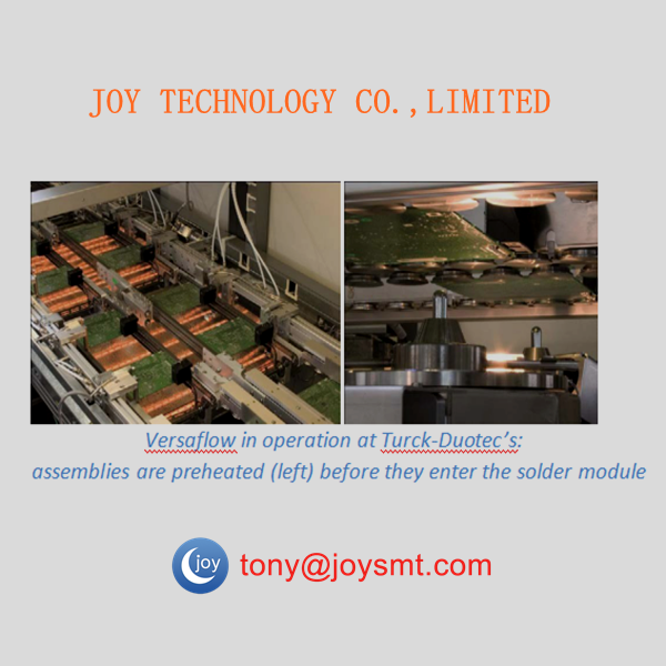
The production island solution chosen with the selective soldering systems offers very short processing times. The special in-line concept of the VERSAFLOW allows for simultaneous processing of three assemblies in the system. Fluxing, preheating and soldering are concurrently taking place in the corresponding modules. The cycle time of the system is therefore short, depending only on the number of solder joints to be made. Since long distances to move assemblies from module to module are dispensed with, processing times of app. 3x the cycle time of one assembly are achieved. The total production time for low volume orders is therefore, when compared to a traditional wave soldering process, substantially shorter.
Another large benefit of the VERSAFLOW 3 is its modularity, which the system retains even though it may already be installed at the customers site.
Now in its 3rd generation, it offers higher productivity and flexibility while reducing its footprint and lowering its operating cost.
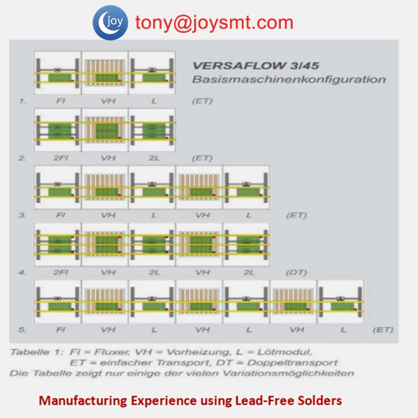
Through the new modular platform, the system requires, when compared to its precursors, substantially less floor space. An in-line selective soldering system consists, in its basic configuration, of a fluxer, a preheat and a soldering module, with a segmented conveyor transporting the boards. Depending on the application and the throughput requirements, an additional solder pot, fluxer and/or preheat modules can be retrofitted into the system at the customer site. Together with the requirements of the customer, the system can grow along with his needs.
The smallest configuration is the fluxer, preheat, solder module version. The maximum configuration foreseen is a fluxer, 3 preheat modules and 3 solder modules. This configuration, though, could be doubled when specifying the optional dual track. This “dual track” option was adapted from the reflow sector. It allows for a doubling of the throughput while retaining the floor space required, meaning that up to 22 individual assemblies can be parallel processed in the system at the same time. Only the usable board width is reduced accordingly. The axis system of the xyz-table remains. In the case of the dual-track option, the xyz-tables will be equipped with a second solder bath. This means that on each xyz-axis system, two solder baths operate in parallel.
The smaller process window, the existence of which became apparent during our initial process trials, has been confirmed by our experience during regular, every day production. A process qualification is therefore vital, and experience shows that the optimization phase for new assemblies using lead-free solder requires more time than the time required for tin/lead solder.
To assure a safe process and to put it on a stable, broad base requires a stringent monitoring effort. Aside from the task of monitoring the temperature profile at regular intervals, it is imperative that a regularly scheduled solder analysis is being performed. Copper and lead are two of the elements which need to be especially closely monitored, as they can contaminate the solder beyond the permissible limits rather quickly. This analysis is recommended to be done in intervals of 4 weeks, especially at the beginning and until a pattern has been established.
The contamination of the solder through lead will hopefully eliminate itself in the near future; already today it does not pose a real danger any longer.
Copper leaching, on the other hand, is not going to go away by itself, and remains an issue which will require continued attention. The leaching of copper into lead-free solder is contingent on the solder temperature, the dynamic of the solder wave and the alloy itself. Regardless of these noted conditions, the rate of dissolution is in all cases higher than the leaching experienced in tin/lead solders. The accumulation of the copper in the solder bath causes a shift of the solder composition away from the eutectic. That gives rise to the formation of an alloy that does not exhibit the abrupt and well defined transition between solid and liquid and its reverse, but exhibits a range during which transition takes place, a range which stretches in line with the amount of copper present. This transition range is characterized by the appearance of intermetallic CuSn needles (dendrites), which segregate in the still liquid solder. When now the component lead breaks out of the solder and the solder joint formed begins to cool down, this dendritic solidification may be the cause for an increase in the defect rate experienced. Icicles and bridging may be the visual result.
Having qualified personnel available is extremely important if problems of this type are to be avoided. Through adequate training and instructions it has to be learned to recognize which process indicators are important, and which preventative measures are appropriate to take to keep the process stable. Yet, this training is only the beginning, and it is the kick-off for a very valuable chain of experiences gleaned during regular production, experiences, which cannot be substituted by anything.
For products, for which a superior quality and a high level of reliability are called for, hand soldering cannot provide the required degree of repeatability which can be realized with an automated mass soldering process. In instances where operating costs have to be reduced, or where mixed technology boards with a high density of SMD components need to be processed, standard wave soldering may not be a viable solution either, especially in a lead-free process. Unavoidable higher operating costs due to the increased maintenance requirement, the increase in dross generated and the more frequent need to analyze the solder alloy would be a consequence of this process. The high cost for N2 and for the attendant rework due to the higher defect rate needs to be added as well. All these factors speak for a change from wave soldering over to the selective soldering process. The process advantages “better, faster, cleaner & more cost effective” that characterize the VERSAFLOW selective soldering systems do not only provide for a substantial improvement in the quality of the product, they do so also at a significantly reduced operating cost.


 Panasonic CM202 CM402 CM602 NPM Nozzle 110 115 KXFX0383A00
 Samsung SM320 IC tray
 YAMAHA FEEDER CALIBRATION JIG