How Does 3D AOI Increase Manufacturing Quality?
PCB suppliers in the automotive space are vastly accelerating their time to market by using automated optical inspection (AOI) systems during PCB assembly. However, this next‐generation technique is not limited in scope to the automotive industry – it has powerful implications for the entire PCB industry.
What is 3D AOI?
To best understand the benefits that 3D AOI offers, it's useful to compare it to its predecessor, 2D AOI. In the past, automated optical inspection processes allowed electronics manufacturers to identify workmanship defects and other issues during the final stages of PCB assembly.
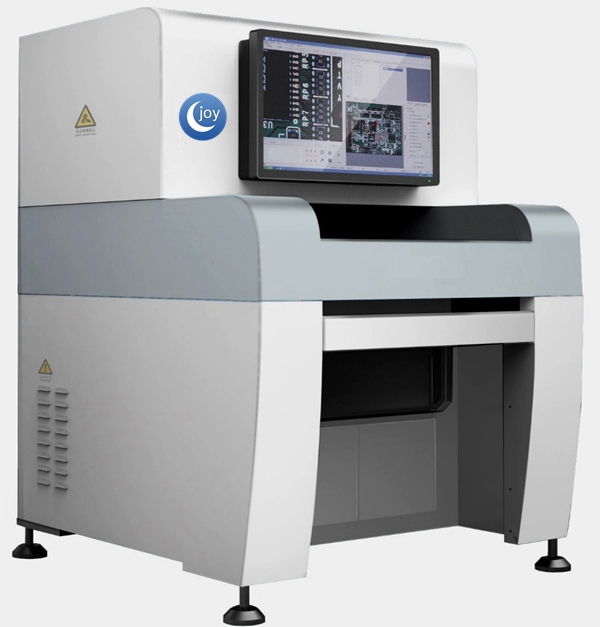
AOI Equipment
In a typical AOI setting, a top‐mounted camera takes precisely measured photographs of finished circuit boards and compares the results to a highly detailed schematic file. Parameter differences that pass a certain threshold get flagged, and a human operator inspects the product in question.
The upshot of this process is that human operators no longer need to manually verify every parameter of a finished circuit board – for modern PCBs, that would take far too long. Now, a small team of operators can verify a very large volume of PCBs and pick out the defective ones with great accuracy.
3D AOI builds on this premise by using two cameras to develop a three‐dimensional image of the PCB. This allows the AOI process to verify smaller components than ever before. In some cases, the addition of a side‐mounted stereo camera set lets the optical image technology build a complete render of the PCB, allowing for unprecedented precision and quality control.
Who Uses 3D AOI for PCB Inspection?
As of mid‐2017, this technology is almost exclusively used in the autonomous vehicles industry. The ability to quickly identify and measure panel defects when dealing with extremely small components is an important factor contributing towards making autonomous vehicles an everyday reality.
However, as time goes on, this inspection process will become more commonplace, vastly reducing the time and energy spent on PCB inspection. Manufacturers are continually looking for better, more efficient test methods that offer real‐time feedback. This way, PCB defects can be identified early in the manufacturing process, saving customer grief and company reputation by preventing potential recalls or, in some industry sectors, lawsuits.
When combined with laser direct imaging (DI) technology, AOI improves yield by minimizing expensive material waste. The combination increases the traceability of the supply chain and helps manufacturers identify the factors that generate production failures.


 Panasonic CM202 CM402 CM602 NPM Nozzle 110 115 KXFX0383A00
 Samsung SM320 IC tray
 YAMAHA FEEDER CALIBRATION JIG