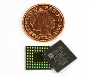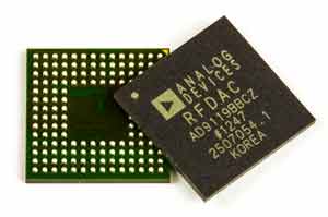
A Ball Grid Array or BGA package is a form of surface mount technology, or SMT package that is being used increasingly for integrated circuits.
The BGA offers many advantages and as a result it is being used increasingly in the manufacture of electronic circuits.
The Ball Grid Array, BGA package was developed out of the need to have a more robust and convenient package for integrated circuits with large numbers of pins. With the levels of integration rising, some integrated circuits had in excess of 100 pins.

The conventional quad flat pack style packages had very thin and close spaced pins, and these were very easy to damage, even in a controlled environment. Additionally they required very close control of the soldering process otherwise the level of solder bridges and poor joints rose. From a design viewpoint, the pin density was such that taking the tracks away from the IC also proved to be problematic as there could be congestion in some areas. The BGA package was developed to overcome these problems, and improve reliability from the soldered joints.
The Ball Grid Array was developed to provide a number of benefits to IC and equipment manufacturers as well as providing benefits to the eventual users of equipment. Some of the BGA benefits over other technologies include:
These advantages have meant that despite initial scepticism about the package, it provides some useful improvements in many circumstances..
The Ball Grid Array, BGA, uses a different approach to the connections to that used for more conventional surface mount connections. Other packages such as the quad flat pack, QFP, used the sides of the package for the connections. This meant that there was limited space for the pins which had to be spaced very closely and made much smaller to provide the required level of connectivity. The Ball Grid Array, BGA, uses the underside of the package, where there is a considerable area for the connections.

The pins are placed in a grid pattern (hence the name Ball Grid Array) on the under-surface of the chip carrier. Also rather than having pins to provide the connectivity, pads with balls of solder are used as the method of connection. On the printed circuit board, PCB, onto which the BGA device is to be fitted there is a matching set of copper pads to provide the required connectivity.
Apart from the improvement in connectivity, BGAs have other advantages. They offer a lower thermal resistance between the silicon chip itself than quad flat pack devices. This allows heat generated by the integrated circuit inside the package to be conducted out of the device onto the PCB faster and more effectively. In this way it is possible for BGA devices to generate more heat without the need for special cooling measures.

In addition to this the fact that the conductors are on the underside of the chip carrier means that the leads within the chip are shorter. Accordingly unwanted lead inductance levels are lower, and in this way, Ball Grid Array devices are able to offer a higher level of performance than their QFP counterparts.
In order to meet the variety of requirements for different types of assembly and equipment, a number of BGA variants have been developed.