
Joy Technology Co.,Limited
SMT Equipment∣SMT parts∣SMT Solution provider


Ball grid arrays are the boon and bane of engineers and printed circuit board designers the world over. Their unparalleled pin density and low lead inductance are essential in today’s high pin count, high frequency integrated circuits. However, that same pin density and unique interface create a challenge unique unto themselves. These challenges need to be faced head on since the ball grid array (BGA)is prevalent in modern PCBs. While there are entire textbooks that cover the topic of BGAs, their use and fanout techniques, the quick overview provided here offers an engineer a good starting point for improving BGA designs.
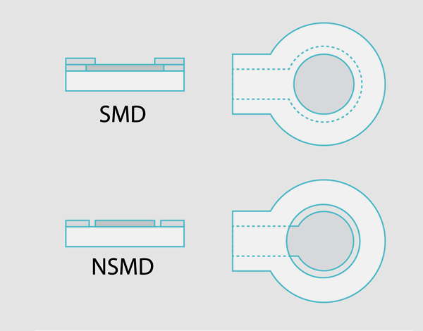
While the basic BGA concept has remained the same, they have been changing in dimensions since their introduction, with smaller pitches and smaller outlines. Certain BGAs have no connections in the center, while others have pins all across the bottom of the package. For simpler BGAs, with greater pitch and space
in the middle of the BGA, manual routing can be accomplished without creating a breakout pattern. As the pitch decreases and pin count goes up, the amount of connections required makes the semi-random placement of traces unfeasible. While increasing layers of the board can be a shortcut to make it simpler to route the traces, this creates increased cost and greater reliability concerns, which should be avoided. If it is possible to reduce the layer requirements by more thoughtful layouts, then do so, only increasing the layer count as a last option.
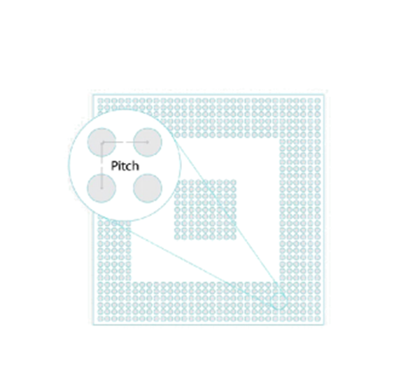
As the different ball patterns on the board give rise to different optimal fanouts or escape routing, it’s important to carefully look at
the patterns and ask various questions. How far apart are the balls. Are they parallel and equidistant, or do they have greater spacing in one direction. Does the pattern change.
What is your minimum trace width and spacing.
Advanced Assembly was founded to help engineers assemble their prototype and low-volume PCB orders. Based on years of experience within the printed circuit board industry, Advanced Assembly developed a proprietary system to deliver consistent, machine surface mount technology (SMT) assembly for 1-35 boards in 1-5 days. It’s our only focus. We take the hassle out of PCB assembly and make it easy, so you can spend time on other aspects of your design.
 Panasonic CM202 CM402 CM602 NPM Nozzle 110 115 KXFX0383A00
 Samsung SM320 IC tray
 YAMAHA FEEDER CALIBRATION JIG