How to quickly remove plastic ball grid array package (PBGA) from pcb board
How to remove the plastic ball grid array package (PBGA) from the printed circuit board (PCB), which is the necessary skills for every hardware division. ADI gives a set of recommended rework procedures for removing the PBGA package from the PCB.
PBGA is a package, the main distinguishing feature is the use of solder ball array to contact with the substrate (such as PCB). This feature gives the PBGA an advantage of configuring different packages (such as single, double, four, and four) with respect to other pins, which is the ability to achieve higher pin densities. The internal interconnection of the PBGA package is achieved by wire bonding or flip chip technology. The PBGA chip containing the integrated circuit is packaged in a plastic material.
PBGA Device Rework After the PBGA device is assembled to the PCB, if defect is found, it should be reworked to remove the defective device and replace it with a working device. Before removing the device, the defective device should be heated until the solder joint is liquefied to remove undesirable devices from the board.
The routine rework procedure is as follows
Prepare the board
Remove the device
Clean the PCB pad
Coated with solder paste
Device alignment and patch
Fixed device
an examination
Introduce the above seven steps before the first to say that remove the device and the attention of the thing.
When removing the device, mechanical stress may be generated on PBGA and / or PCB. Care should be taken to remove defective devices, to avoid damage to the PCB, adjacent devices and defective devices themselves, especially if the user intends to analyze the defective device.
If there is excessive stress on the PBGA device, such as heating the device above the rated peak temperature or overly exposed to high temperatures, it may result in packaging delamination or external physical damage (see Figures 2 and 3). For further analysis of the device, the removal caused by the improper layer will increase the difficulty of finding the real failure mechanism. Therefore, in order to carry out effective fault analysis, proper removal of defective devices is necessary.
Prepare the board
It is strongly recommended that the PCB components be dry before the start of the repair to eliminate residual moisture. If it is not removed, the residual moisture may be damaged during the reflow due to the "popcorn effect". Bake the PCB assembly at 125 ° C for at least 4 hours as long as these conditions do not exceed the rated limits of other devices on the PCB. If these conditions exceed the rated limits of other devices, the optional baking conditions described in the Joint Industry Standard IPC / JEDEC J-STD-033 should be used.
Remove the device
You can use different tools to remove the device. In order to remove the device, it may be necessary to heat the device until the solder reflows and then remove the device by mechanical means when the solder is still in the liquid state. The programmable hot air repair system provides controlled temperature and time settings. Rework should follow the temperature profile used for device assembly. The repair temperature must not exceed the peak temperature specified on the humidity sensitivity rating (MSL) label. The heating time can be shortened (for example, for the liquefaction zone) as long as the solder is completely reflowed. The solder reflow zone should be at a peak temperature of less than 60 seconds. The vacuum pressure of the pick-up tool should be less than 0.5 kg / cm2 to prevent the device from erecting before full reflow, and to avoid wiping the pad. Do not use devices removed from the PCB.
Control the repair temperature to avoid damage to PBGA devices and PCBs. It should be considered that the heating rate of the PBGA may be faster than the lead-based package, such as standard outline integrated circuit (SOIC) and leadframe chip-scale package (LFCSP) due to thermal quality. Note that it is possible to provide further protection by covering the area around the device with a heat-resistant tape. In addition, it is recommended to heat the PCB below to reduce the temperature difference between the upper and lower sides of the PCB, the board bending the smallest.
When setting the rework tool setting, the temperature curve should be calibrated. This calibration is particularly important when you first rework a particular device. The PBGA devices are also calibrated using different body sizes, solder compositions, or different PCB materials, configurations, sizes and thicknesses, as they may have different thermal mass values.
The calibration must include monitoring the temperature, time, and other settings of the device tool (see Figure 4). The thermocouple should be fitted to different parts of the board assembly, such as the upper part of the PBGA device and the upper part of the PCB (see Figure 5). Analyze the time and temperature curve data, and obtain the valid parameters removed from the evaluation.
A simplified flow chart for device removal evaluation
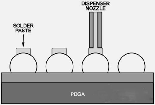
Figure 5. Device removal calibration setting diagram
Clean the PCB pad
After removing the PBGA device, the solder on the PCB will have too much solder and must be cleaned before installing the replacement PBGA device. Pad cleaning can be divided into two steps:
Go to tin Use solder lines and blade-type soldering iron to remove excess solder on the pad (see Figure 6). The width of the selected blade should match the maximum width occupied by the device. The blade temperature must be low enough to avoid damage to the circuit board. Flux can be applied to the pad, and then remove the solder and remove the excess solder.
Figure 6. PCB pad to tin
clean. Clean the area with a cleaning agent on the rework area and wipe it with a lint-free cloth. The cleaning agent used depends on the type of solder paste used in the original assembly.
Coated with solder paste
The solder paste should be applied prior to mounting the replacement PBGA device on the circuit board to replace the solder paste applied to the original circuit board to ensure the reliability of the PBGA welded joint. The amount of solder paste applied to each solder ball must be consistent so that the PBGA is not coplanar when the circuit board is installed.
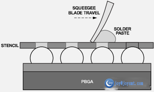
A template can be used to apply the solder paste to the PCB pad. The alignment accuracy of the template is the key to keeping reflow soldering evenly. Use the same PBGA aperture geometry and template thickness as the board assembly. Use a trapezoidal aperture (see Figure 7) to ensure uniform release of the solder paste and reduce blemishes.
Template aperture geometry (A is longer than B)
In some cases, it may not be possible to apply the solder paste evenly and precisely on the PCB pad with a template, especially for circuit boards with high device density or geometric space. In this case, consider applying solder paste to the solder balls at the bottom of the device. For this purpose, the solder paste can be applied to the top of the solder ball using a template or the solder paste is dispensed to all solder balls (see Figures 8 and 9). This can be achieved with specially designed fixtures and / or rework equipment.
The solder paste template prints the solder paste onto the solder ball
Place the solder paste on the solder ball
Device alignment and patch
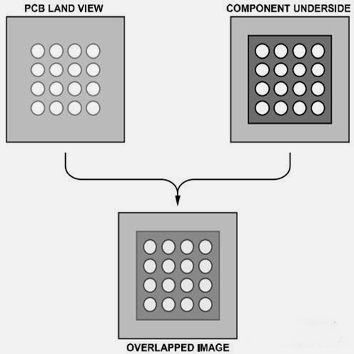
It is important to place the device precisely on the board. Chip devices with sub-beam optical systems help align PBGA and circuit boards. This type of imaging system involves mirroring the PBGA ball image on the PCB pad image (see Figure 10). The placement machine must have the ability to support the user to fine-tune (including rotation) along the x-axis and y-axis.
Align the PCB and device with a sub-beam optical system
The accuracy of the patch depends on the equipment or process used. Although PBGA packages are often aligned automatically during reflow, make sure that the patch deviation is less than 50% of the PCB pad width. If the alignment error is too large, the solder bridge may cause electrical short circuit.
Fixed device
Since all reflow parameters have been optimized, the thermal curve developed during the original assembly process should be used.
Examination
After reflow, check the assembled PBGA for defects, such as misalignment or damage. Use X-ray to check for problems such as solder bridges and tin beads. If necessary, perform an electrical verification test to verify that the device is functioning properly


 Panasonic CM202 CM402 CM602 NPM Nozzle 110 115 KXFX0383A00
 Samsung SM320 IC tray
 YAMAHA FEEDER CALIBRATION JIG