
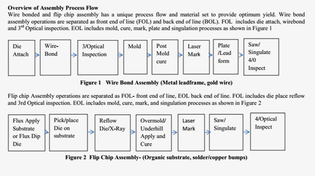
Joy Technology Co.,Limited
SMT Equipment∣SMT parts∣SMT Solution provider


Defects and failure mode evaluation
The package manufacturing process has a variety of materials and processes used to make the end product. There can be many sources of defects if materials and processes are not controlled adequately. One key defect prevention tool used in the early engineering stages is DFMEA ( Design Failure Modes and Effects analysis) and PFMEA ( Process Failure Modes and Effects Analysis) to predict the risks in design and process and put controls in place to minimize defects
The migration to thin form factor packages requires more focus on handling controls, moisture sensitivity classifications,[3], material shelf life and tighter process windows.
The flip chip package assembly yields are very dependent on proper bump alignment, reflow and molding process. The laminate substrate material, surface finish, and CTE play a key role in the reliability of the package. Successful assembly of the package requires proper bump alignment and intermetallic formation at package /die interface and bump/substrate interface as shown in Figure 11 and Figure 12. The laminate pad geometry and solder mask windows optimization is critical for proper joint formation. The glass transition temperature of the laminate, and its CTE (Coefficient of thermal expansion) and warpage characteristics can have an impact on bump reliability. Additionally, reflow profiles need to be optimized to provide adequate solder reflow without causing delamination of the substrate.
Proper pad to bump alignment is more critical for a copper stud bump as it does not have the self-centering that a solder bump has. CTE mismatch between substrate and die can have significant impact on copper bump reliability. [4].Figure 13 shows an acceptable joint using copper interconnect and Figure 14 shows a crack in a copper bump interconnect.
X-sectioning is conducted post reflow to understand the solder joint profile, alignment, presence or absence of voids and to evaluate the grain structure of the solder joint. Voids can get trapped at the bump to substrate interface and cause assembly issues. Generally acceptable criteria for voids are less than 30% of the bump diameter.
Switching to a low voiding solder paste can help minimize the void issue. An alternate to bumping with solder paste is a solder ball drop process which has minimal void issues.
X- Sectional analysis also helps evaluate the package molding process to ensure that there is proper coverage of the mold compound around the bumps and minimal voiding. Low pin count packages are typically over molded and survive the package level reliability tests. Higher pin counts packages require under fill apply and cure post reflow. Careful l evaluation of under filled packages is required to ensure that there is no solder extrusion in the under fill during the cure process. Other failure modes that can be seen in X-sectional and SEM/EDX analysis are UBM (under bump metallurgy) separation from solder bump, passivation cracking, bump corrosion, pad separation etc.
The variety of defects discussed earlier in flip chip and wire bonded packages require a thorough follow up with production line records, controls, training and documentation. Typical causes of cosmetic and functional defects are optimized processes, handling damage, ESD controls, operator turnover, training, material controls etc. Some of the defects are not exposed during qualification process and surface later on when machines and processes are fully utilized for prodcution ramp. To minimize this defect escape a detailed package contstruction analysis is condcuted prior to qualification approval. The allows time to isolate defects and drive corrective action and conduct process window optimization before launching production.
For wire bonded packages, die attach , ball bonds, wedge bonds and package molding are evaluated using a X-section. Figure 15 shows the package wire bonds and Figure 16 shows the package mold compound.
Wirebond reliability is critcal for the success of the package in assembly processes and subsequent customer applicatios. Proper intermetallic formation and shear values >25 gms, and minimal voiding are expected post wire bond. Figure17 shows the intermetallic formation in agold to Aluminum wire bond. Figure 18 shows a wedge bond made on the lead. Lifted wedge bonds can be prevented by optimizing the bond parameter recipes and maintaining a clean bond surface.
X-sectional analysi s is also conducted for flip chip package to understand the package an ddie thicness, laminate, vias, bump height, voids , intermetallics etc. Figure 19 shows a X-section of a flip chip package.
The controls on the production floor or at asubcontract operation need tobe reviewed frequently to minimze defect occurrence and escape. When a failure mode is understood and corrected, the FMEAS and control plans should be updated to reflect the changes and the “lessons learned”. Yield targets and yield improvement plan should be defined prior to prodcution launch
As originally published in the IPC APEX EXPO Conference Proceedings.
and reviewed on an ongoing basis. Yield data review using top 3 yield detractors by part number is helpful in DPPM reduction efforts. Manufacturing line audits and training review and refresher are also a means for continuous improvement. Monitoring Cp/Cpk for each critcal process and 10- 15 production lots after launch provides an effective source of issues to focus for continuous proces improvement and optimization.
Conclusion:
Wire bonded and flip chip bu mped interconnects are a reliable form of interconnect if bond parameters, reflow process, mold material sets, substrate pads and solder mask are optimized. Successful assembly and reliability of these packages can be achieved with careful understanding of failure modes, clear ,concise documentation, training and teamwork with subcontract facilities.
 Panasonic CM202 CM402 CM602 NPM Nozzle 110 115 KXFX0383A00
 Samsung SM320 IC tray
 YAMAHA FEEDER CALIBRATION JIG